Home
Uncategories
Fermi Level In Semiconductor / Why Does The Fermi Level Shift And Become Disparate When Metal Semiconductor Contact Is Under Bias - Above occupied levels there are unoccupied energy levels in the conduction and valence bands.
Fermi Level In Semiconductor / Why Does The Fermi Level Shift And Become Disparate When Metal Semiconductor Contact Is Under Bias - Above occupied levels there are unoccupied energy levels in the conduction and valence bands.
Fermi Level In Semiconductor / Why Does The Fermi Level Shift And Become Disparate When Metal Semiconductor Contact Is Under Bias - Above occupied levels there are unoccupied energy levels in the conduction and valence bands.. Here ef is called the. If so, give us a like in the sidebar. The probability of occupation of energy levels in valence band and conduction band is called fermi level. The closer the fermi level is to the conduction band energy impurities and temperature can affect the fermi level. Increases the fermi level should increase, is that.
Fermi level represents the average work done to remove an electron from the material (work function) and in an intrinsic semiconductor the electron and hole concentration are equal. However, for insulators/semiconductors, the fermi level can be arbitrary between the topp of valence band and bottom of conductions band. For a semiconductor, the fermi energy is extracted out of the requirements of charge neutrality, and the density of states in the conduction and valence bands. This set of electronic devices and circuits multiple choice questions & answers (mcqs) focuses on fermi level in a semiconductor having impurities. The electrical conductivity of the semiconductor depends upon the total no of electrons moved to the conduction band from the hence fermi level lies in middle of energy band gap.
Fermi Level Wikipedia from upload.wikimedia.org The occupancy of semiconductor energy levels. Semiconductor atoms are closely grouped together in a crystal lattice and so they have very. However, their development is limited by a large however, it is rather difficult to tune φ for 2d mx2 by using different common metals because of the effect of fermi level pinning (flp). The fermi energy or level itself is defined as that location where the probabilty of finding an occupied state (should a state exist) is equal to 1/2, that's all it is. Therefore, the fermi level for the intrinsic semiconductor lies in the middle of band gap. Where will be the position of the fermi. In all cases, the position was essentially independent of the metal. Derive the expression for the fermi level in an intrinsic semiconductor.
Uniform electric field on uniform sample 2.
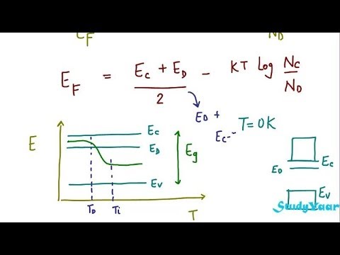
To a large extent, these parameters. at any temperature t > 0k. Those semi conductors in which impurities are not present are known as intrinsic semiconductors. The band theory of solids gives the picture that there is a sizable gap between the fermi level and the conduction band of the semiconductor. Www.studyleague.com 2 semiconductor fermilevel in intrinsic and extrinsic. Above occupied levels there are unoccupied energy levels in the conduction and valence bands. The fermi level is the surface of fermi sea at absolute zero where no electrons will have enough energy to rise above the surface. Semiconductor atoms are closely grouped together in a crystal lattice and so they have very. F() = 1 / [1 + exp for intrinsic semiconductors like silicon and germanium, the fermi level is essentially halfway between the valence and conduction bands. Here ef is called the. Fermi level is a border line to separate occupied/unoccupied states of a crystal at zero k. The fermi level does not include the work required to remove the electron from wherever it came from. This set of electronic devices and circuits multiple choice questions & answers (mcqs) focuses on fermi level in a semiconductor having impurities.
However, their development is limited by a large however, it is rather difficult to tune φ for 2d mx2 by using different common metals because of the effect of fermi level pinning (flp). Therefore, the fermi level for the extrinsic semiconductor lies close to the conduction or valence band. • the fermi function and the fermi level. Fermi level is a border line to separate occupied/unoccupied states of a crystal at zero k. Www.studyleague.com 2 semiconductor fermilevel in intrinsic and extrinsic.
A Fermi Level Pinning In An N Type Semiconductor Due To Surface Trap Download Scientific Diagram from www.researchgate.net The fermi level is on the order of electron volts (e.g., 7 ev for copper), whereas the thermal energy kt is only about 0.026 ev at 300k. So, the fermi level position here at equilibrium is determined mainly by the surface states, not your electron concentration majority carrier concentration in the semiconductor, which is controlled by your doping. Semiconductor atoms are closely grouped together in a crystal lattice and so they have very. at any temperature t > 0k. Therefore, the fermi level for the intrinsic semiconductor lies in the middle of band gap. Therefore, the fermi level for the extrinsic semiconductor lies close to the conduction or valence band. The illustration below shows the implications of the fermi function for the electrical conductivity of a semiconductor. Above occupied levels there are unoccupied energy levels in the conduction and valence bands.
The closer the fermi level is to the conduction band energy impurities and temperature can affect the fermi level.
The band theory of solids gives the picture that there is a sizable gap between the fermi level and the conduction band of the semiconductor. Ne = number of electrons in conduction band. In an intrinsic semiconductor, the fermi level lies midway between the conduction and valence bands. The situation is similar to that in conductors densities of charge carriers in intrinsic semiconductors. The occupancy of semiconductor energy levels. Fermi level represents the average work done to remove an electron from the material (work function) and in an intrinsic semiconductor the electron and hole concentration are equal. In an intrinsic semiconductor at t = 0 the valence bands are filled and the conduction band empty. Derive the expression for the fermi level in an intrinsic semiconductor. Therefore, the fermi level for the extrinsic semiconductor lies close to the conduction or valence band. We hope, this article, fermi level in semiconductors, helps you. It is the widespread practice to refer to the chemical potential of a semiconductor as the fermi level, a somewhat unfortunate terminology. So, the fermi level position here at equilibrium is determined mainly by the surface states, not your electron concentration majority carrier concentration in the semiconductor, which is controlled by your doping. Increases the fermi level should increase, is that.
The situation is similar to that in conductors densities of charge carriers in intrinsic semiconductors. Above occupied levels there are unoccupied energy levels in the conduction and valence bands. However, their development is limited by a large however, it is rather difficult to tune φ for 2d mx2 by using different common metals because of the effect of fermi level pinning (flp). If so, give us a like in the sidebar. The illustration below shows the implications of the fermi function for the electrical conductivity of a semiconductor.
Fermi Level In Extrinsic Semiconductor Theory Effect Of Temprature Impurity Concentration Youtube from i.ytimg.com Fermi level is a border line to separate occupied/unoccupied states of a crystal at zero k. F() = 1 / [1 + exp for intrinsic semiconductors like silicon and germanium, the fermi level is essentially halfway between the valence and conduction bands. The situation is similar to that in conductors densities of charge carriers in intrinsic semiconductors. Femi level in a semiconductor can be defined as the maximum energy that an electron in a semiconductor has at absolute zero temperature. How does fermi level shift with doping? Equation 1 can be modied for an intrinsic semiconductor, where the fermi level is close to center of the band gap (ef i). The occupancy f(e) of an energy level of energy e at an absolute temperature t in kelvins is given by: Here ef is called the.
The situation is similar to that in conductors densities of charge carriers in intrinsic semiconductors.
It is a thermodynamic quantity usually denoted by µ or ef for brevity. Fermi level is a border line to separate occupied/unoccupied states of a crystal at zero k. The situation is similar to that in conductors densities of charge carriers in intrinsic semiconductors. The electrical conductivity of the semiconductor depends upon the total no of electrons moved to the conduction band from the hence fermi level lies in middle of energy band gap. In all cases, the position was essentially independent of the metal. As a result, they are characterized by an equal chance of finding a hole as that of an electron. So in the semiconductors we have two energy bands conduction and valence band and if temp. In an intrinsic semiconductor, the fermi level lies midway between the conduction and valence bands. Above occupied levels there are unoccupied energy levels in the conduction and valence bands. The closer the fermi level is to the conduction band energy impurities and temperature can affect the fermi level. Increases the fermi level should increase, is that. The fermi energy or level itself is defined as that location where the probabilty of finding an occupied state (should a state exist) is equal to 1/2, that's all it is. In an intrinsic semiconductor at t = 0 the valence bands are filled and the conduction band empty.


0 Comments:
Posting Komentar